
सीएसआईआर-राष्ट्रीय भौतिक प्रयोगशाला
CSIR-National Physical Laboratory

Quantum Nanophotonics Metrology
About Activity/ Objective
The group is working towards the realization of quantum devices based on superconducting nanowires and junctions.
Development of Superconducting Nanowire Single Photon Detectors (SNSPD)
The superconducting nanowire single photon detector (SNSPD) is capable of detection of single photons with wide wavelength range. SNSPDs have unrivalled performance indicators compared to the traditional technologies such as Si-APDs and InGaAs-APDs in terms of detection efficiency (DE), timing jitter, reset time, and dark count rates (DCR). A detection efficiency of ~ 98% and timing jitter of ~ 10 ps are demonstrated in lab level for system such as WSi and NbTiN with superconducting transition temperature of ~4 K and 15 K respectively. As the photon detection mechanisms in SNSPDs are based on the conversion of the superconducting state to normal state and vice versa upon the impinge of a photon, these detectors are to be operated at cryogenic temperatures (~2K -10 K). Another advantageous factor for the SNSPDs is the range of wavelengths these detectors are sensitive to: this spans from infrared to visible and even the researchers have shown the detection of alpha and beta particles with SNSPDs. Such a wide wavelength sensitivity is not available with traditional technologies. In the demanding applications of quantum technologies such as quantum information processing, quantum communication, teleportation and quantum computation, the incorporation of SNSPDs can provide unparalleled performance levels as compared to the traditional technologies.
SNSPD consists of superconducting nanowire shaped in the form of mender wires with an individual wire width of 40-120 nm and thickness of ~ 4-10 nm and with an active area of the detector with a few square micrometers. Upon the impinge of a photon the device produces an electrical pulse as the outcome with a response time (jitter timing) of ~10 ps. The reset time of the device is ~ 100 ns, after which the device is ready for detection of another photon. Carefully crafted detectors can also be used as photon counting detectors and photon number resolving (PNR) detectors. CSIR-National Physical Laboratory with its expertise on superconductivity and thin film fabrication have demonstrated superconducting characteristics in meander structures such as Nb, NbGd and W (focused ion beam fabricated) with a transition temperature in the range from ~4 K to 8 K. We also have demonstrated superconductivity in the 2D regime for system such as Nb, NbTiN, TiN etc. which is a critical requirement for the development of SNSPDs. Further, we would like to use the available expertise to develop, demonstrate and standardise the SNSPDs to cater the current and future needs of the country towards quantum enabled technologies such as quantum information processing (QIP), quantum key distribution (QKD), quantum computation, and quantum communication etc. With the support from DST (QuEST Project) and CSIR(FCP) we are currently engaged in capability building of single photon detectors and its standardisation methods using superconducting nanowires.
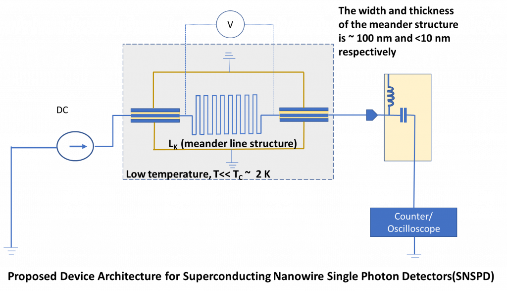
The picture given below shows a schematic of the proposed device architecture for the SNSPD development. The key components include the room temperature biasing circuit, the SNSPD device operated at cryogenic temperature (typically ~2 K) and the room temperature detector electronics. Single photon generation for testing this device is through attenuation of the laser source down to very low levels and further evaluation by statistical methods to ensure that the output is of the level of single photons as per the required pulsed rate.
Development of Quantum Phase Slip (QPS) based Quantum Current Standard (QCS) using Superconducting Nanowires (QPS-QCS)
One of the unsolved problems in electrical metrology is the realisation of the current standard (Ampere) to the uncertainty levels as that has been demonstrated for the quantum voltage standard (JVS) for voltage and quantum Hall resistance standard (QHR) for resistance. Metrological community is working to solve this issue using different methods such Single Electron Tunnelling (SET) based devices and quantum phase slip (QPS) based devices. QPS devices are exactly dual to Josephson devices wherein, upon the irradiation of the microwave radiation to a superconducting nanowire in the voltage biased mode, will produce constant current plateaus as function of the incident energy(frequency). So, the current I can be defined as I= 2e.n.f, where ‘e’ charge of the electron, and ‘f’ is the frequency of irradiation, ‘n’ being an integer. As per the new definition of the SI unit of electrical current, which came into force from May 2019 onwards, all the realisations of the definition of the SI unit of electric current should define experiments for the measurements of electron charge. Thus, QPS in superconducting nanowires is one of the promising methods for the realisation of the “Quantum Ampere”.
The main objectives under this activity are the following:
- Establishment of quantum current standard (QCS) by using quantum phase slip (QPS)in superconducting nanowire
- Fundamental research on quantum transport in low dimensional superconductors
The above-mentioned objectives are further divided into mainstream research areas as listed below:
- Fundamental R&D work on the establishment of quantum current by quantum phase slip (QPS) mechanism with the following steps:
(i) Synthesis and structural characterization of high-quality superconducting thin films and composite materials by UHV magnetron sputtering unit
(ii) Fabrication of thin films based superconducting devices and their low temperature transport characterization
(iii) Patterning thin films into nanowire, meander and other various nanostructures for the possible use in QPS and other high impedance circuits required for the quantum current metrology and QPS study
(iv) Characterization of the superconducting nanodevices at ultra-low temperature down to 10-20 mK and at high magnetic field up to 14 T
- Quantum transport in low dimensional superconductors with emphasis on the following phenomena:
(i) Superconducting fluctuations: Phase and amplitude fluctuations
(ii) Superconductor-insulator quantum phase transition (SIT)
(iii) Quantum interference
(iv) Multiple crossing in magnetoresistance for strongly disordered ultrathin superconducting films in 2D
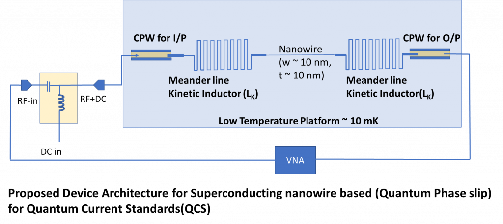
The following figure represents a simplified schematic device architecture for realisation of QPS based quantum current standard. A superconducting nanowire of cross-sectional area of ~100 nm2 needed to be sandwiched between two impedance matched inductors for RF irradiation experiments along with DC biasing. The proposed device is to be tested at ultra-low temperature of the order of a few mK, so that the thermal noises are suppressed enough for the manifestation of QPS signals.
Dissemination of the Unit of Voltage through Programmable Josephson Voltage Standard (PJVS)
At CSIR-NPL, we disseminate the unit of voltage through a programmable Josephson voltage standard (PJVS) which is being maintained with an uncertainty level of below 100 nV (for 10 V)
Salient Features of the Established PJVS System are:
- This system is superior to the conventional JVS system because of its stable steps, higher susceptible to interference, easier to operate and provide more possibilities and applications in ac voltage.
- The 10 V chip contains a total of 256,116 Josephson junctions organised in stacks of three junctions and distributed into 32 microwave coplanar waveguide lines.
- These non-hysteretic Josephson tunnel junctions are made of Nb electrodes and NbxSi1-x barriers.
- Array with 256,116 triple stacked SNS junctions, all connected in series and integrated in a microwave transmission line (upto 20 GHz).
- Essential role in electrical metrology and high precision voltage measurement.
The Programmable Josephson Voltage Standard, established at CSIR-NPL is characterized for its optimal functioning to disseminate ‘Unit’ Volt at par to international level. This optimization in the characterization of the system has ensured us to operate the system consistently and with better stability and reproducibility.
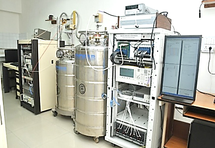
Established PJVS system at CSIR-NPL India for quantum DC voltage metrology
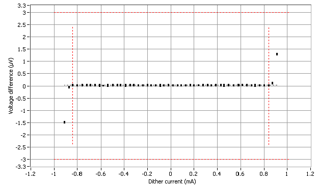
Step flatness test at 18.645 GHz and 0.00 dBm
This system provides calibration services to disseminate the primary voltage standard. The 10 V PJVS system is capable of providing traceability at 1.018 V and 10 V levels. This system is primarily used for the calibration of dc reference standards which serves as secondary standard of voltage for further dissemination to industries.
CMC
This group maintains two number of CMCs at 1.018 V and 10 V levels mentioned with Institution Service code as NPLI/1-2 registered in BIPM.
Facilities
- Focused Ion-Beam Milling
- Dilution Refrigerator (10 mK, 14 Tesla)
- UHV Sputtering System
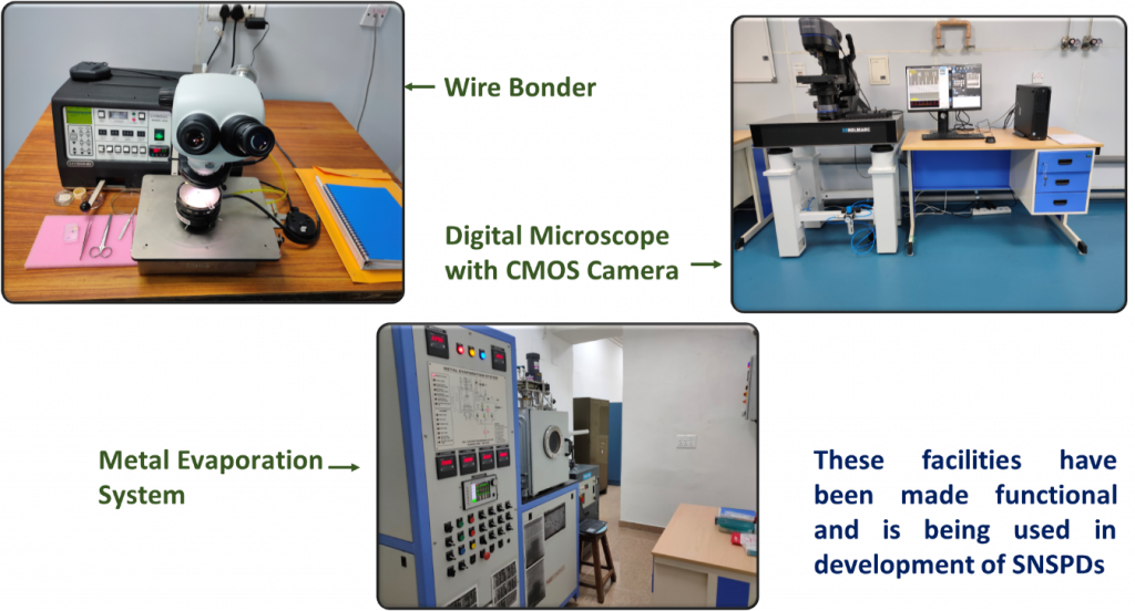
- Wire Bonder
- Digital Microscope with CMOS Camera
- Metal Evaporation system
Key Publications (Last 5 years)
- Deepika Sawle, Sudhir Husale, Sachin Yadav, Bikash Gajar, V.P.S. Awana and Sangeeta Sahoo*, “Accessing Phase Slip Events in Nb Meander Wires”, Superconductor Science & Technology, 34, 125016 (2021)
- Sachin Yadav, Vinay Kaushik , M. P. Saravanan , R. P. Aloysius, V. Ganesan and Sangeeta Sahoo*, “A robust nitridation technique for fabrication of disordered superconducting TiN thin films featuring phase slip events”, Scientific Reports, 11, 7888 (2021)
- Sachin Yadav and Sangeeta Sahoo*, “Interface study of thermally driven chemical kinetics involved in Ti/Si3N4 based metal-substrate assembly by X-ray photoelectron spectroscopy”, Applied Surface Science, 541, 148465 (2021)
- Bikash Gajar, Sachin Yadav, Deepika Sawle, Kamlesh K. Maurya, Anurag Gupta, R.P. Aloysius, and Sangeeta Sahoo*, “Substrate mediated nitridation of niobium into superconducting Nb2N thin films for phase slip study”, Scientific Reports, 9, 8811 (2019)
- Sachin Yadav, Alka Sharma, Bikash Gajar, Mandeep Kaur, Dinesh Singh, Sandeep Singh, Kamlesh Kumar Maurya, Sudhir Husale, Vijay Narain Ojha, Sangeeta Sahoo*, “Substrate Mediated Synthesis of Ti–Si–N Nano-and-Micro Structures for Optoelectronic Applications”, Advanced Engineering Materials, 21, 1900061 (2019). $The story of the above article has been appeared on the cover page of the journal’s issue from July, 2019
- Shafaq Kazim, Alka Sharma, Sachin Yadav, Bikash Gajar, Lalit M. Joshi, Monu Mishra, Govind Gupta, Sudhir Husale, Anurag Gupta, Sangeeta Sahoo* & V. N. Ojha, “Light Induced Electron-Phonon Scattering Mediated Resistive Switching in Nanostructured Nb Thin Film Superconductor”, Scientific Reports 7, 881 (2017)
- Anish M. Bhargav, Rajib K. Rakshit, Samaresh Das, and Manju Singh, “Metrology Perspective of Single-photon Detectors: Review on Global Calibration Methods” [‘Advanced Quantum Technologies’ – Wiley, https://doi.org/10.1002/qute.202100008]
Current R &D Projects
- DST project: Advanced Single Photon Detector & Establishment of Single Photon Detection Based Quantum Standard for QuEST)
- CSIR Grant for setting up of low temperature experimental facility towards the establishment of single photon detection-based quantum metrology for optical radiation.
Team
Dr. R.P. Aloysius
Sr. Principal Scientist & Head
Quantum Nanophotonics Metrology
Email: alosrp.nplindia@csir.res.in
Dr. Sangeeta Sahoo
Sr. Principal Scientist & Deputy Head
Quantum Nanophotonics Metrology
Email: sahoos.nplindia@csir.res.in
Dr. Sudhir Husale
Sr. Principal Scientist
Email: husalesc.nplindia@csir.res.in
Dr. Sandhya Malikar Patel
Principal Scientist
Email: patelsm.nplindia@csir.res.in
Ms. Mandeep Kaur
Technical Officer
Email: kaurm.nplindia@csir.res.in
Sh. Anish Mahavir Bhargav
Technical Officer
Email: bhargavam.nplindia@csir.res.in
Contact Person
Dr. R.P. Aloysius
Sr. Principal Scientist & Head
Quantum Nanophotonics Metrology
Electrical & Electronics Metrology Division
Email: alosrp.nplindia@csir.res.in
All Rights Reserved - The Official Website of CSIR-National Physical Laboratory, CSIR, under Ministry of S & T, Govt. of India
Site Designed & Managed by Knowledge Resource Centre
CSIR-NPL, New Delhi
India